Back End Domains
IEEE Major Projects Backend Domains
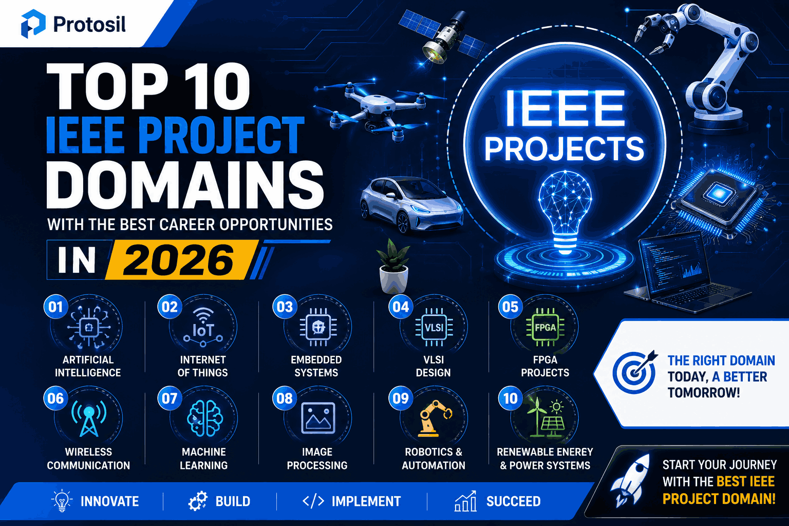
Backend design plays a critical role in VLSI and semiconductor engineering, focusing on the physical implementation, optimization, power management, and performance enhancement of integrated circuits. IEEE Major Projects Backend Domains help students gain practical exposure to advanced chip design methodologies, low-power architectures, memory systems, and nanoscale technologies that are widely used in modern semiconductor industries. The Takeoff page primarily focuses on backend VLSI domains such as Low Power VLSI, Core Memories, Transistor Logic, Nano Technology, and Cadence-based implementation environments.
At Protosil, we help students develop innovative IEEE Major Projects Backend Domains that align with current semiconductor industry requirements and emerging research trends. These projects are suitable for B.Tech, M.Tech, ECE, EEE, and VLSI specialization students looking to build expertise in chip design and hardware implementation.
Popular IEEE Backend Project Domains
Low Power VLSI Projects
Low Power VLSI is one of the most important research areas in modern semiconductor design due to increasing demand for energy-efficient electronic devices.
Popular project areas include:
- Low Power CMOS Design
- Energy-Efficient Processor Architectures
- Power Optimization Techniques
- Battery-Efficient Embedded Systems
- Memory Power Reduction Methods
Low-power architectures continue to be widely adopted in mobile devices, IoT systems, and embedded applications.
Core Memory Projects
Memory systems are essential components of modern digital devices and computing architectures.
Students can explore:
- SRAM Design and Optimization
- Memory Controller Architectures
- Cache Memory Systems
- High-Speed Memory Design
- Low-Power Memory Structures
Core memory projects help students understand storage architectures, memory efficiency, and semiconductor implementation techniques.
Transistor Logic Projects
Transistor logic remains a fundamental area in VLSI design and digital electronics.
Project domains include:
- CMOS Logic Design
- Logic Gate Optimization
- High-Speed Digital Circuits
- Power-Aware Logic Architectures
- Advanced Logic Implementations
These projects provide strong exposure to circuit-level design and optimization methodologies.
Nano Technology Projects
Nanotechnology is increasingly being integrated into semiconductor and VLSI design to improve performance, scalability, and power efficiency.
Students can work on:
- CNTFET-Based Designs
- Nano VLSI Architectures
- QCA-Based Systems
- Nano Memory Structures
- Nanoscale Computing Applications
Nano Technology is one of the backend domains highlighted within IEEE VLSI project categories due to its growing research significance.
Cadence EDA Projects
Cadence EDA tools are widely used for circuit design, verification, simulation, and backend implementation.
Popular project areas include:
- Physical Design Flow
- Layout Design and Verification
- Timing Analysis
- Design Rule Checking
- Backend Optimization Techniques
Industry-standard EDA tools help students understand professional semiconductor design workflows.
Why Choose IEEE Backend Domain Projects?
IEEE backend projects provide practical exposure to semiconductor technologies, chip design methodologies, and advanced hardware implementation techniques. Since these projects are based on current research and industry practices, they help students develop valuable technical and analytical skills.
Key benefits include:
- Semiconductor design exposure
- Practical VLSI implementation experience
- Strong research foundation
- Better placement opportunities
- Industry-relevant technical skills
- Preparation for higher studies and R&D careers
How Protosil Helps Students
Backend VLSI projects often require expertise in design tools, simulation environments, and hardware implementation methodologies. At Protosil, we provide complete guidance to help students successfully complete their IEEE backend projects.
Our support includes:
- IEEE project topic selection
- Research paper analysis
- Cadence EDA guidance
- Simulation and verification support
- Documentation assistance
- Technical mentoring and consultation
We help students build practical projects that align with modern semiconductor industry requirements and academic expectations.
Why Choose Protosil?
Students choose Protosil because of our commitment to quality project development and technical excellence.
- Latest IEEE backend project domains
- Research-oriented project guidance
- Expert technical mentoring
- Industry-focused implementation support
- Customized project assistance
- End-to-end project development support
Our objective is to help students gain practical semiconductor design experience while developing strong technical foundations for future careers.
Frequently Asked Questions - IEEE Major Projects
IEEE Major Projects Backend Domains focus on physical design, Low Power VLSI, Core Memories, Transistor Logic, Nano Technology, and semiconductor implementation techniques.
Low Power VLSI, Core Memories, Transistor Logic, Nano Technology, and Cadence EDA-based projects are among the most popular backend domains.
Yes. Backend projects are widely selected by B.Tech and M.Tech students interested in semiconductor design, physical implementation, and chip optimization.
Cadence EDA, Tanner EDA, H-Spice, LT-Spice, Xilinx Vivado, and FPGA development platforms are commonly used.
Yes. Protosil provides complete guidance for IEEE backend domain projects, including topic selection, implementation support, simulation assistance, and project documentation.
Always Smart To Hear News
Our Latest Blog